
LTCC was originally developed from multi-layer capacitor fabrication technology. Fabrication commences with the manufacture of the ceramic material from a mixture of organic and inorganic materials to form a thin flexible tape. At this stage the ceramic substrate material is said to be in its “green state” and is quite fragile. Each LTCC component is fabricated from multiple tape layers processed in parallel to form a multi-layer ceramic “sandwich”. Different patterning of metals and resistive materials on the separate layers allows the design of complex functionality within the LTCC component. Component manufacture commences with the blank green tape ceramic material being cut in to tiles of the required size (typically 100-mm square). Vias and cavities are then punched in the blank tiles and the vias filled with conductive paste. The required conductor pattern is then printed with conductive pastes (also called “inks”). Resistive inks can also be printed to form integral resistors. These processes are all carried out in parallel for each of the different layers of the LTCC component. Once all of the layers have been completed and checked they are collated in to a stack. They are then laminated under pressure and sintered at around 850°C. The laminated stack is finally sawn and the individual pieces are available for component assembly and test.

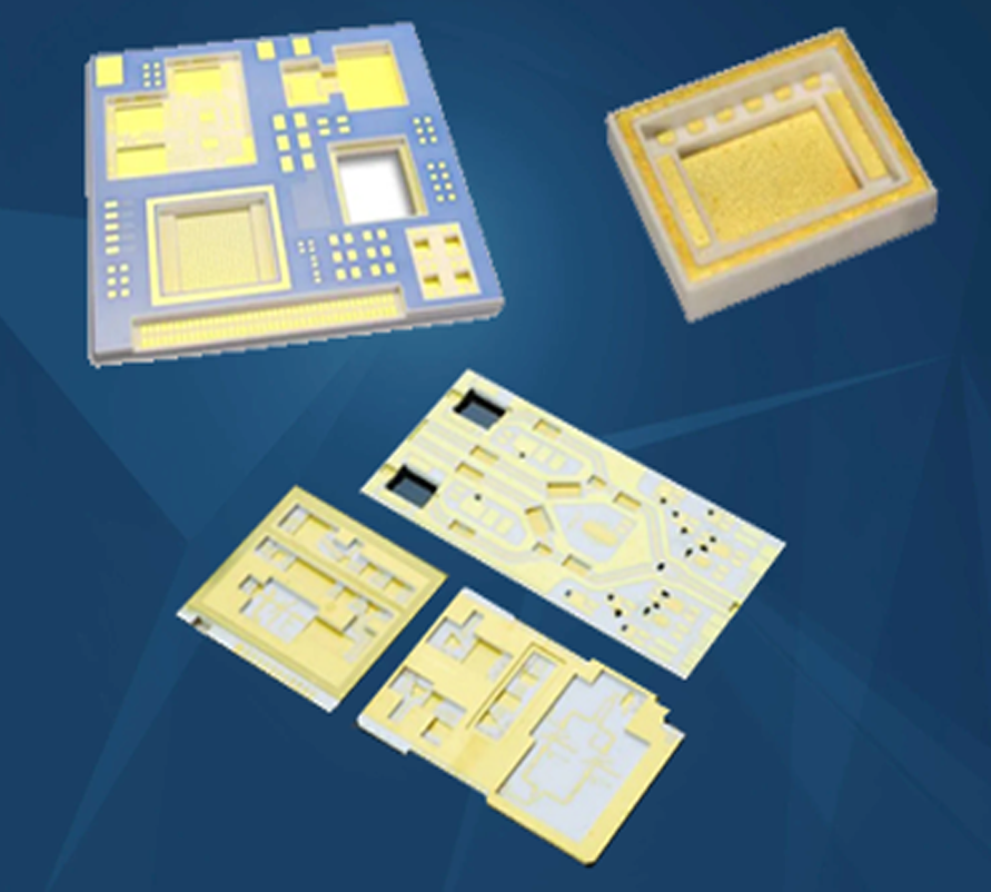
Low Temperature Co-Fire Ceramics (LTCC) Substrates
Low Temperature Co-Fire Ceramics (LTCC) Substrates
LTCC stands for Low Temperature Co-Fired Ceramic and refers to a process for the production of ceramic multilayer circuits. By printing the individual ceramic layers, conductive paths, resistors and capacitive and inductive functionalities can be created.
LTCC Capabilities
-
Substrate Size: 100 mmx 100 mm maximum
-
Minimum Line width and spacing : 0.15mm
-
Conductor Thickness : 10 to 20micron
-
Through hole diameter :0.1 mm
-
Print accuracy :±10 micron
-
Stack Alignment Accuracy: 5 to30 micron
-
Shrinkage : 2%
-
Resistor size : 0.3mmx0.3mm