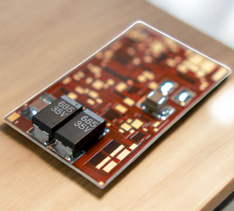
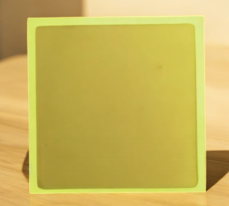
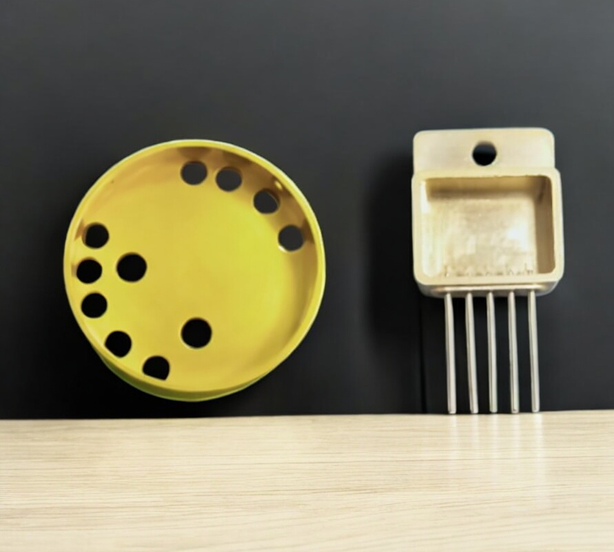
Direct Copper Bonding Substrates (DCBS) means process in which copper sheet is directly bonded on a ceramic substrate such as Al2O3 (aluminium oxide). Direct copper bonded substrates have been proven for many years as an excellent solution for electrical isolation and thermal management of high power semiconductor modules. Al2O3 (aluminium oxide) serving as an insulating layer, and copper connections to ensure the electrical conductivity at high temperatures.
The advantages of DBC substrates are high current carrying capability due to thick copper metallization and a thermal expansion close to the silicon at the copper surface due to high bond strength of copper to ceramic DCBS substrates have an excellent performance/cost efficiency ratio. The great heat conductivity of Al2O3 (24 W/mK) as well as the high heat capacity make it classic irreplaceable in power electronics. The thick copper foils offer extremely good electrical and thermal conductivity and form an outstanding base for the soldering and wire bonding processes.


